(1) Mechanical grinding
(2) Chemical mechanical planarization
(3) Wet etching
(4) Plasma Dry Chemical Etching (ADP DCE)
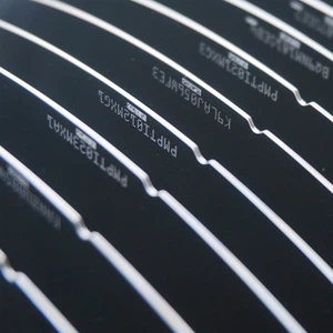
Mechanical (Conventional) Grinding – This process has a high rate of thinning, making it a very common technique. It uses a diamond and resin-bonded grinding wheel mounted on a high-speed spindle, similar to those used in spin-coating applications. The grinding recipe determines the speed of the spindle as well as the material removal rate.
The process is a two-step process:
1. Coarse grinding does most of the refining at a rate of ~5μm/sec.
2. Fine grinding with 1200 to 2000 grit and poligrind. Typically removes ~30µm of material at a rate of Less than or equal to 1µm/sec and provides a final finish on the wafer.
The 1200-grit has a rough finish with noticeable wear marks, while the 2000-grit is less rough but still has some wear marks. Poligrind is a polishing tool that provides maximum wafer strength and removes most subsurface damage.
1. Mount the wafer on a backside membrane, such as a wax holder, to hold it in place.
2. Apply the chemical slurry from above and distribute it evenly with a polishing pad.
3. Rotate the polishing pad for approximately 60-90 seconds per buff, depending on final thickness specifications.
Liquid etchants vary depending on the desired thickness and whether isotropic or anisotropic etching is desired. In isotropic etching, the most common etchant is a combination of hydrofluoric acid, nitric acid, and acetic acid (HNA). The most common anisotropic etchants are potassium hydroxide (KOH), ethylenediaminecatechol (EDP) and tetramethylammonium hydroxide (TMAH). Most reactions proceed at a rate of ~10 μm/min, and the reaction rate may vary depending on the etchant used in the reaction.
ADP DCE is the latest wafer thinning technology, similar to wet etching. Instead of using liquids, dry chemical etching uses plasma or etchant gases to remove material. To perform the thinning process, a beam of highly kinetic particles can be fired at the target wafer, chemicals react with the wafer surface, or both are combined. The removal rate of dry etching is about 20μm/min, and there is no mechanical stress or chemicals, so this method can produce very thin wafers with high quality.
Jul 01, 2023השאר הודעה

